Keyboard shortcuts

Press ← or → to navigate between chapters

Press S or / to search in the book

Press ? to show this help

Press Esc to hide this help

Pulse Width Modulation (PWM)

PWM Introduction

Pulse-width modulation (PWM) is a method for using pulse width to encode or modulate a signal. The width of each pulse is a function of the amplitude of the signal.

Duty Cycle

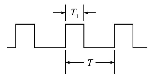
The duty cycle is measured in percentage. The percentage duty cycle specifically describes the percentage of time a digital signal is on over an interval or period of time. This period is the inverse of the frequency of the waveform.

PWM waveform showing the period T and the pulse width T1 of a square signal

  • T: Tx_THRESHOLD register configuration
  • T1: Tx_TH_CHANNELx register configuration

Clock Source

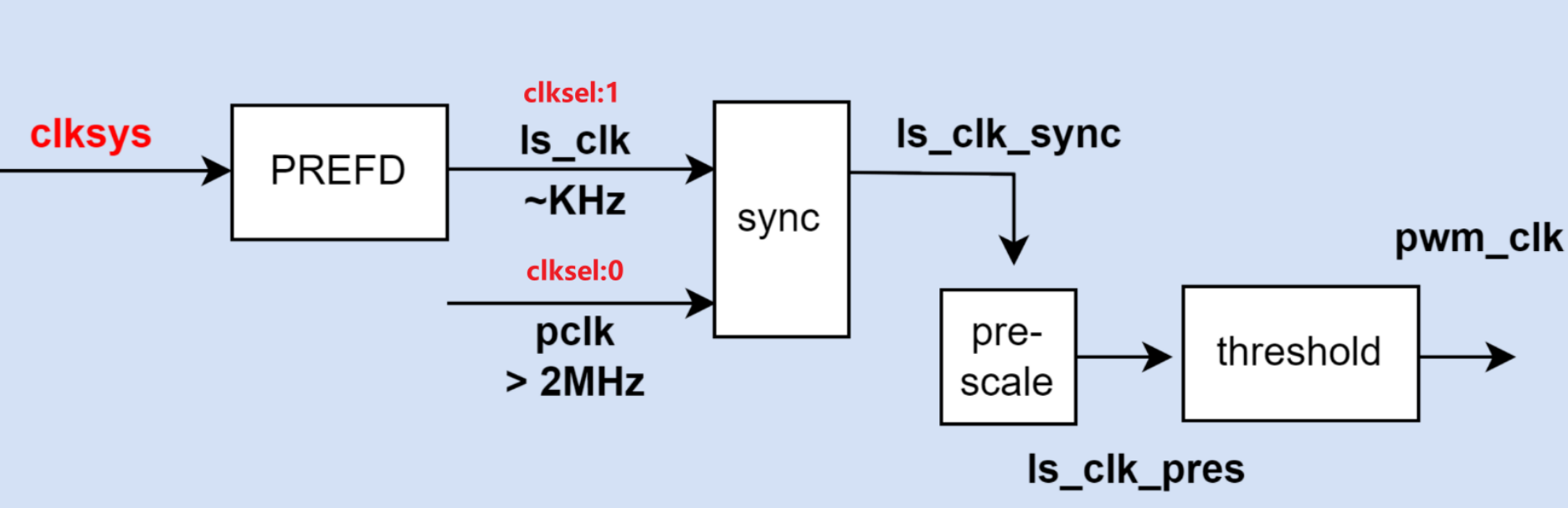
The PWM supports 2 different input sources, configured by the Tx_CONFIG registers. The clock gates are controlled by the CG register.

PWM clock path: clksys through the PREFD divider (clksel 1, ls_clk) or pclk above 2 MHz (clksel 0) into the sync block, then the pre-scale stage (ls_clk_pres) and the threshold stage, producing pwm_clk

Example: how to generate a clock frequency of 5 Hz from the PWM output pin:

T2_CONFIG    = (1 << 11) | (1 << 12) | (0x30 << 16);  // prescale 48, T2_CONFIG[11] = 0x1 (is_clk)
T2_PREFD     = 0x03E8 (1000)
T2_THRESHOLD = 0x64 (100)
  • ls_clk = 48 MHz / (2 × T2_PREFD) = 48 MHz / 2000 = 24 kHz
  • ls_clk_pres = 24 kHz / 48 = 500 Hz
  • pwm_clk = 500 Hz / 100 = 5 Hz

PWM Main Features

  • 16-bit resolution
  • Multiple pulse width output modes
  • 4 timers for PWM
  • 4 channels for every timer
  • Each channel is independently configured with a duty cycle
  • GPIO trigger mode:
    • Trigger event on input source rising edge
    • Trigger event on input source falling edge
    • Trigger event on input source falling or rising edge

PWM Interrupts

The PWM module generates 4 events or interrupts:

  • Event: the event signal is asserted when the counter reaches the threshold (TH) of the channel.
  • Each timer independently generates an event.

PWM interrupts IRQn table:

PWMNVIC IRQn
T0140
T1141
T2142
T3143

PWM Registers

Base address: 0x5012_0000

Register NameOffsetSizeTypeAccessDefaultDescription
T0_CMD0x000032ConfigR/W0x00000000Command
T0_CONFIG0x000432ConfigR/W0x00000000Configuration
T0_THRESHOLD0x000832ConfigR/W0x00000000Threshold configuration
T0_TH_CHANNEL00x000C32ConfigR/W0x00000000Channel 0 threshold configuration
T0_TH_CHANNEL10x001032ConfigR/W0x00000000Channel 1 threshold configuration
T0_TH_CHANNEL20x001432ConfigR/W0x00000000Channel 2 threshold configuration
T0_TH_CHANNEL30x001832ConfigR/W0x00000000Channel 3 threshold configuration
T0_COUNTER0x002C32StatusR0x00000000Counter
T1_CMD0x004032ConfigR/W0x00000000Command
T1_CONFIG0x004432ConfigR/W0x00000000Configuration
T1_THRESHOLD0x004832ConfigR/W0x00000000Threshold configuration
T1_TH_CHANNEL00x004C32ConfigR/W0x00000000Channel 0 threshold configuration
T1_TH_CHANNEL10x005032ConfigR/W0x00000000Channel 1 threshold configuration
T1_TH_CHANNEL20x005432ConfigR/W0x00000000Channel 2 threshold configuration
T1_TH_CHANNEL30x005832ConfigR/W0x00000000Channel 3 threshold configuration
T1_COUNTER0x006C32StatusR0x00000000Counter
T2_CMD0x008032ConfigR/W0x00000000Command
T2_CONFIG0x008432ConfigR/W0x00000000Configuration
T2_THRESHOLD0x008832ConfigR/W0x00000000Threshold configuration
T2_TH_CHANNEL00x008C32ConfigR/W0x00000000Channel 0 threshold configuration
T2_TH_CHANNEL10x009032ConfigR/W0x00000000Channel 1 threshold configuration
T2_TH_CHANNEL20x009432ConfigR/W0x00000000Channel 2 threshold configuration
T2_TH_CHANNEL30x009832ConfigR/W0x00000000Channel 3 threshold configuration
T2_COUNTER0x00AC32StatusR0x00000000Counter
T3_CMD0x00C032ConfigR/W0x00000000Command
T3_CONFIG0x00C432ConfigR/W0x00000000Configuration
T3_THRESHOLD0x00C832ConfigR/W0x00000000Threshold configuration
T3_TH_CHANNEL00x00CC32ConfigR/W0x00000000Channel 0 threshold configuration
T3_TH_CHANNEL10x00D032ConfigR/W0x00000000Channel 1 threshold configuration
T3_TH_CHANNEL20x00D432ConfigR/W0x00000000Channel 2 threshold configuration
T3_TH_CHANNEL30x00D832ConfigR/W0x00000000Channel 3 threshold configuration
T3_COUNTER0x00EC32StatusR0x00000000Counter
EVENT_CFG0x010032ConfigR/W0x00000000Events configuration
CG0x010432ConfigR/W0x00000000Channels clock gating configuration
T0_PREFD0x014032ConfigR/W0x0000000032M clock frequency division for timer 0
T1_PREFD0x014432ConfigR/W0x0000000032M clock frequency division for timer 1
T2_PREFD0x014832ConfigR/W0x0000000032M clock frequency division for timer 2
T3_PREFD0x014C32ConfigR/W0x0000000032M clock frequency division for timer 3

Register Descriptions

Tx_CMD — Command Register

  • Address offset: 0x00X0 (T0 X=0; T1 X=4; T2 X=8; T3 X=C)
  • Reset value: 0x0000_0000
BitsFieldDescription
[1]STOPStop command bitfield
[0]STARTStart command bitfield

Tx_CONFIG — Configuration Register

  • Address offset: 0x00X4 (T0 X=0; T1 X=4; T2 X=8; T3 X=C)
  • Reset value: 0x0000_0000
BitsFieldDescription
[23:16]PRESCPrescaler value configuration. Value = actual value − 1
[12]UPDOWNSELCenter-aligned mode configuration: 0 = the counter counts up and down alternately; 1 = the counter counts up and resets to 0 when reaching the threshold
[11]CLKSELClock source configuration: 0 = pclk, 1 = is_clk
[10:8]MODETrigger mode configuration bitfield: 000 = trigger event at each clock cycle; 001 = trigger event if input source is 0; 010 = trigger event if input source is 1

Tx_THRESHOLD — Threshold Configuration Register

  • Address offset: 0x00X8 (T0 X=0; T1 X=4; T2 X=8; T3 X=C)
  • Reset value: 0x0000_0000
BitsFieldDescription
[31:16]TH_HIThreshold high part configuration bitfield. It defines the end counter value.
[15:0]TH_LOThreshold low part configuration bitfield. It defines the start counter value.

Note: Value = actual value − 1

Tx_TH_CHANNEL0 — Channel 0 Threshold Configuration Register

  • Address offset: 0x00XC (T0 X=0; T1 X=4; T2 X=8; T3 X=C)
  • Reset value: 0x0000_0000
BitsFieldDescription
[18:16]MODEChannel 0 threshold match action on channel output signal configuration bitfield: 000 = set; 001 = toggle, then next threshold match action is clear; 010 = set, then next threshold match action is clear; 011 = toggle; 100 = clear; 101 = toggle, then next threshold match action is set; 110 = clear, then next threshold match action is set
[15:0]THChannel 0 threshold configuration bitfield. Value = actual value − 1
Tx_TH_CHANNEL1 — Channel 1 Threshold Configuration Register

  • Address offset: 0x00X0 (T0 X=1; T1 X=5; T2 X=9; T3 X=D)
  • Reset value: 0x0000_0000
BitsFieldDescription
[18:16]MODEChannel 1 threshold match action on channel output signal configuration bitfield: 000 = set; 001 = toggle, then next threshold match action is clear; 010 = set, then next threshold match action is clear; 011 = toggle; 100 = clear; 101 = toggle, then next threshold match action is set; 110 = clear, then next threshold match action is set
[15:0]THChannel 1 threshold configuration bitfield. Value = actual value − 1
Tx_TH_CHANNEL2 — Channel 2 Threshold Configuration Register

  • Address offset: 0x00X4 (T0 X=1; T1 X=5; T2 X=9; T3 X=D)
  • Reset value: 0x0000_0000
BitsFieldDescription
[18:16]MODEChannel 2 threshold match action on channel output signal configuration bitfield: 000 = set; 001 = toggle, then next threshold match action is clear; 010 = set, then next threshold match action is clear; 011 = toggle; 100 = clear; 101 = toggle, then next threshold match action is set; 110 = clear, then next threshold match action is set
[15:0]THChannel 2 threshold configuration bitfield. Value = actual value − 1

Tx_TH_CHANNEL3 — Channel 3 Threshold Configuration Register

  • Address offset: 0x00X8 (T0 X=1; T1 X=5; T2 X=9; T3 X=D)
  • Reset value: 0x0000_0000
BitsFieldDescription
[18:16]MODEChannel 3 threshold match action on channel output signal configuration bitfield: 000 = set; 001 = toggle, then next threshold match action is clear; 010 = set, then next threshold match action is clear; 011 = toggle; 100 = clear; 101 = toggle, then next threshold match action is set; 110 = clear, then next threshold match action is set
[15:0]THChannel 3 threshold configuration bitfield. Value = actual value − 1

Tx_COUNTER — Counter Register

  • Address offset: 0x00XC (T0 X=2; T1 X=6; T2 X=A; T3 X=E)
  • Reset value: 0x0000_0000
BitsFieldDescription
[31:0]CounterRead: value of the T0/1/2/3 counter

EVENT_CFG — Events Configuration Register

  • Address offset: 0x0100
  • Reset value: 0x0000_0000
BitsFieldDescription
[19]EN3Enable T3 event generation
[18]EN2Enable T2 event generation
[17]EN1Enable T1 event generation
[16]EN0Enable T0 event generation
[15:12]T3chselT3 event source selection configuration bitfield: 0xC = T3 channel 0; 0xD = T3 channel 1; 0xE = T3 channel 2; 0xF = T3 channel 3
[11:8]T2chselT2 event source selection configuration bitfield: 0x8 = T2 channel 0; 0x9 = T2 channel 1; 0xA = T2 channel 2; 0xB = T2 channel 3
[7:4]T1chselT1 event source selection configuration bitfield: 0x4 = T1 channel 0; 0x5 = T1 channel 1; 0x6 = T1 channel 2; 0x7 = T1 channel 3
[3:0]T0chselT0 event source selection configuration bitfield: 0x0 = T0 channel 0; 0x1 = T0 channel 1; 0x2 = T0 channel 2; 0x3 = T0 channel 3

CG — Channels Clock Gating Configuration Register

  • Address offset: 0x0104
  • Reset value: 0x0000_0000
BitsFieldDescription
[3:0]enClock gating configuration bitfield: 0 = clock gated, 1 = enabled. Bit[0] = T0 configuration; Bit[1] = T1 configuration; Bit[2] = T2 configuration; Bit[3] = T3 configuration

Tx_PREFD — Clock Frequency Division Configuration Register

  • Address offset: 0x014X (T0 X=0; T1 X=4; T2 X=8; T3 X=C)
  • Reset value: 0x0000_0000
BitsFieldDescription
[9:0]CLK_FD32 MHz clock frequency division: 0, 1 = no division. Value = actual value − 1