Keyboard shortcuts

Press or to navigate between chapters

Press S or / to search in the book

Press ? to show this help

Press Esc to hide this help

System Control (Always-On)

Always-On Domain Overview

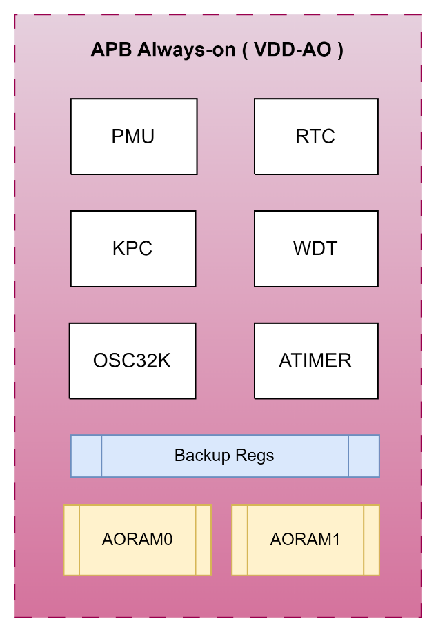
The Always-On (AO) power domain manages the power-on sequence and remains powered in all operating modes until the chip is completely shut down. It handles activity monitoring to wake up the SoC whenever needed, and manages power supply sequencing during initial power-on or any power mode transition.

AO domain block diagram showing PMU, RTC, WDT, ATimer, KPC, BUREG, RAM, and IO PAD blocks

The AO domain contains the following logic blocks:

  • PMU — Power management unit. Controls power domains of the SoC subsystem, manages wake-up triggers to recover from sleep mode, and supports separate trimmings and enables (power-on autoloaded from ReRAM IFR; SW-configurable for debug). See the PMU chapter for full details.
  • KPC — Keypad controller. Supports keypad function and can wake the chip from low-power mode. Activating this overrides PF0 functions for the respective pins.
  • RTC — Real-time clock associated with a 32 kHz oscillator (external XTAL or internal RC).
  • WDT — Watchdog timer. Consistent with the SoC-domain WDT peripheral; see the Watchdog Timer section below.
  • ATimer — Always-on timer. Consistent with the SoC-domain ATimer peripheral; see the ATimer section below.
  • BUREG — Backup registers in AO domain. Contents are retained during SoC power-down. Size: 32 bytes. Located at 0x4006_50000x4006_501F. Wake-up via interrupt will preserve the contents; wake-up by system reset will clear the contents.
  • RAM — AO domain RAM. Contents retained during SoC power-down. Split into 2 blocks. Size: 16 KBytes. Located at 0x5030_00000x5030_3FFF.
  • IO PAD — Port F is the special I/O pad group used in the AO domain. PF[1:0] support GPIO and wakeup. PF[9:2] support GPIO and keypad function but do not support wakeup.
  • Interrupts:
    • IRQ 30: AO domain interrupt entry — keypad async input, keypad synced interrupt, watchdog interrupt, ATimer interrupt, RTC interrupt, watchdog reset (6 sources total).
    • IRQ 31: AO wakeup interrupt entry — same 6 sources as IRQ 30, plus PF[1:0] pad inputs (8 sources total).

AO domain address map:

BlockBase Address
PMU0x4006_0000
RTC0x4006_1000
KPC0x4006_4000
AOBUREG0x4006_5000
AORAM0x5030_0000
WDT0x4004_1000
ATimer0x4004_3000

AORAM Erratum

AORAM data at 0x50300000 and 0x50302000 have chance to be reset to 0 during/after VDD85D and VDD33 power cycle.

Do not use the 32-bit words located at 0x50300000 or 0x50302000 for data storage that must be preserved across deep sleep modes.


PMU

The PMU (Power Management Unit) is part of the AO domain and is responsible for managing all SoC power supplies and power-mode transitions.

Full PMU documentation — including the block diagram, regulator descriptions, power mode control flow, and all AO control register descriptions — is covered in the PMU chapter.


RTC

RTC Introduction

The RTC uses a 1 Hz clock signal (CLK1HZ) to increment a counter in one-second intervals, supporting real-time clock and basic alarm functionality in software.

After reset, values must be written to the Load Register (RTC_LR) and Match Register (RTC_MR). The counter increments by 1 on the rising edge of CLK1HZ. When the counter matches the match register and the interrupt is not masked, an interrupt is generated. The interrupt is cleared by writing 1 to RTC_ICR.

RTC Main Features

  • 32-bit free-running up counter.
  • Programmable 32-bit match compare register.
  • Software-maskable interrupt when counter and match registers are identical.

RTC Interrupt

  • Single maskable interrupt RTCINTR, generated on counter/match equality.
  • Enable or disable via bit [0] of RTC_IMSC.
  • Read mask status from bit [0] of RTC_MIS.
  • Clear by writing 1 to bit [0] of RTC_ICR.
  • IRQn: 30

RTC Registers

Base address: 0x4006_1000

RegisterOffsetSizeTypeAccessDefaultDescription
RTC_DR0x000032CRR0x00000000RTC data register
RTC_MR0x000432CRR/W0x00000000RTC match register
RTC_LR0x000832CRR/W0x00000000RTC load register
RTC_CR0x000C32CRR/W0x00000000RTC control register
RTC_IMSC0x001032CRR/W0x00000000Interrupt mask set/clear
RTC_RIS0x001432CRR0x00000000Raw interrupt status
RTC_MIS0x001832CRR0x00000000Masked interrupt status
RTC_ICR0x001C32CRW0x00000000Interrupt clear register

RTC_DR — RTC Data Register

  • Address offset: 0x0000
  • Access: R
BitsFieldDescription
[31:0]RTC_DataCurrent RTC counter value. Reads return the current value of the running counter.

RTC_MR — RTC Match Register

  • Address offset: 0x0004
  • Access: R/W
BitsFieldDescription
[31:0]RTC_Match32-bit match register. An equivalent match value is derived and compared with the counter in the CLK1HZ domain to generate the interrupt. Reads return the last written value.

RTC_LR — RTC Load Register

  • Address offset: 0x0008
  • Access: R/W
BitsFieldDescription
[31:0]RTC_LoadWrites load a new value into the RTC update logic, from which the new counter value is calculated. Reads return the last written value.

RTC_CR — RTC Control Register

  • Address offset: 0x000C
  • Access: R/W
BitsFieldDescription
[31:1]Reserved. Must be written as 0.
[0]RTC start1 = RTC enabled. Do not write this bit again after enabling or the counter resets to zero. Read returns current RTC running status.

RTC_IMSC — Interrupt Mask Set/Clear Register

  • Address offset: 0x0010
  • Access: R/W
BitsFieldDescription
[31:1]Reserved. Must be written as 0.
[0]Interrupt mask0 = interrupt stopped, 1 = interrupt enabled. Read returns current mask value for RTCINTR.

RTC_RIS — Raw Interrupt Status Register

  • Address offset: 0x0014
  • Access: R
BitsFieldDescription
[31:1]Reserved.
[0]Raw statusRaw interrupt state of RTCINTR before masking. Write has no effect.

RTC_MIS — Masked Interrupt Status Register

  • Address offset: 0x0018
  • Access: R
BitsFieldDescription
[31:1]Reserved.
[0]Masked statusMasked interrupt state of RTCINTR after applying mask. Write has no effect.

RTC_ICR — Interrupt Clear Register

  • Address offset: 0x001C
  • Access: W (write-only)
BitsFieldDescription
[31:1]Reserved.
[0]ClearWrite 1 to clear the RTCINTR interrupt flag. Write 0 has no effect.

KPC (Keypad Controller)

KPC Introduction

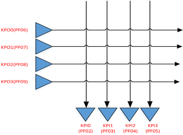
The keypad controller supports a 4×4 keyboard matrix using 4 KPO (output) rows and 4 KPI (input) columns. It monitors the keypad array, detects node rise or fall events, and reports status in KPC_SR.

Note that when the KPC mappings are activated, they will override any GPIO configuration for the PF bank. This also impacts the PA pins that are tied to the PF bank - it is important for the system designer & programmer to ensure no conflicts on these pins, otherwise excessive power draw can result during sleep mode.

For example, if PA0 is configured to drive high, the KPC will drive PF9 (regradless of whether KPO3 is used by the system or not), and this combination will effectively short the high-drive of PA0 onto the KPC’s low-pulse scan of the keyboard matrix.

KPC 4x4 keypad matrix showing KPO rows and KPI columns with node IDs

Node ID mapping:

KPI0KPI1KPI2KPI3
KPO00123
KPO14567
KPO2891011
KPO312131415
  • Port F (PF9–PF2) is dedicated to the keypad function. Use the AO_IOX and AO_PADPU registers for function selection and pull-up configuration.
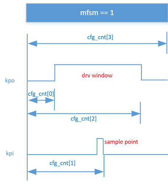
  • Clock source is clk32k, divisible to 1 ms via KPC_CFG1.
  • Keypad sampling timing is configured via KPC_CFG2:

KPC sampling timing diagram showing KPO drive and KPI sample relationships

KPC Main Features

  • Auto-sleep mode; sleep time configured via KPC_CFG4.
  • Each node individually configurable for rise or fall event generation via KPC_CFG3.
  • Multiple simultaneous node events supported via FIFO; indicated in KPC_SR1.
  • Per-node status readable from KPC_SR0.

KPC Interrupt

  • Configure node rise/fall event generation via KPC_CFG3.
  • Enable AO interrupt via the KPCINTR bit in AO_WKUP_INTEN (see PMU).
  • Event flags in KPC_FF.
  • IRQn: 30

KPC Registers

Base address: 0x4006_4000

RegisterOffsetSizeTypeAccessDefaultDescription
KPC_CFG00x000032CRR/W0x0000000DEnable configuration
KPC_CFG10x000432CRR/W0x001F1010Time configuration
KPC_CFG20x000832CRR/W0xFF201810Sample timing configuration
KPC_CFG30x000C32CRR/W0xFFFFFFFFNode event configuration
KPC_SR00x001032SRR0x00000000Status register 0
KPC_SR10x001432SRR0x00000000Status register 1
KPC_FF0x002032CRW0x00000000Event FIFO
KPC_CFG40x003032CRR/W0x000001F4Sleep wait time configuration

KPC_CFG0 — KPC Enable Configuration Register

  • Address offset: 0x0000
  • Reset value: 0x0000_000D
BitsFieldDescription
[5]autosleep enableAuto-sleep enable
[4]kpc enableKPC enable
[3]KPOOE1KPO output enable
[2]KPOOE0KPO output disable
[1]KPOPO1KPO pull-up enable
[0]KPOPO0KPO pull-up disable

KPC_CFG1 — KPC Time Configuration Register

  • Address offset: 0x0004
  • Reset value: 0x001F_1010
BitsFieldDescription
[23:16]Cfg_cnt1msTimer configuration for 1 ms @ clk32k
[15:8]Cfg_filterFilter value, based on mfsm round
[7:0]Cfg_stepBasic time unit

KPC_CFG2 — KPC Sample Timing Configuration Register

  • Address offset: 0x0008
  • Reset value: 0xFF20_1810
BitsFieldDescription
[31:24]cfg_cnt3Time interval between each KPOx line
[23:16]cfg_cnt2Time to stop driving KPOx
[15:8]cfg_cnt1Time of KPIx sample point
[7:0]cfg_cnt0Time to start driving KPOx

KPC_CFG3 — KPC Node Configuration Register

  • Address offset: 0x000C
  • Reset value: 0xFFFF_FFFF
BitsFieldDescription
[31:16]Fall event enableBit N enables fall event/interrupt for node N (nodes 0–15)
[15:0]Rise event enableBit N enables rise event/interrupt for node N (nodes 0–15)

KPC_SR0 — KPC Status Register 0

  • Address offset: 0x0010
  • Reset value: 0x0000_0000
  • Access: R
BitsFieldDescription
[19]KPI[3].piKPI3 current input state
[18]KPI[2].piKPI2 current input state
[17]KPI[1].piKPI1 current input state
[16]KPI[0].piKPI0 current input state
[15:0]Node statusCurrent state of keypad nodes 0–15

KPC_SR1 — KPC Status Register 1

  • Address offset: 0x0014
  • Reset value: 0x0000_0000
  • Access: R
BitsFieldDescription
[0]FIFO valid1 = event FIFO contains a valid entry

KPC_FF — KPC Event FIFO Register

  • Address offset: 0x0020
  • Reset value: 0x0000_0000
  • Access: W
BitsFieldDescription
[31:16]evtimingEvent timing in 10 ms units, measured from last event
[4:0]event index015 = node 0–15 rise event; 1631 = node 0–15 fall event

KPC_CFG4 — KPC Sleep Wait Time Configuration Register

  • Address offset: 0x0030
  • Reset value: 0x0000_01F4
BitsFieldDescription
[15:0]cfg_deep10msTimer configuration for 10 ms @ clk32k (auto-sleep wait time)

ATimer

ATimer Main Features

  • 2 general-purpose 32-bit upwards counters (Lo and Hi).
  • Selectable clock source per counter:
    • PCLK
    • 32 kHz always-on clock
  • 8-bit programmable prescaler (divides clock frequency).
  • Counting modes:
    • One-shot: timer stops after the first compare match.
    • Continuous: timer continues counting after a match.
    • 64-bit cascaded: both 32-bit timers used as a single 64-bit timer.

ATimer Interrupts

  • ATimer0 (Lo) IRQn: 27
  • ATimer1 (Hi) IRQn: 28

ATimer Registers

Base address: 0x4004_3000

RegisterOffsetSizeTypeAccessDefaultDescription
TIMER_CFG_LO0x000032CRR/W0x00000000Timer Low configuration
TIMER_CFG_HO0x000432CRR/W0x00000000Timer High configuration
TIMER_CNT_LO0x000832CRR/W0x00000000Timer Low counter value
TIMER_CNT_HO0x000C32CRR/W0x00000000Timer High counter value
TIMER_CMP_LO0x001032CRR/W0x00000000Timer Low comparator value
TIMER_CMP_HO0x001432CRR/W0x00000000Timer High comparator value
TIMER_START_LO0x001832CRR/W0x00000000Start Timer Low
TIMER_START_HO0x001C32CRR/W0x00000000Start Timer High
TIMER_RESET_LO0x002032CRR/W0x00000000Reset Timer Low counter
TIMER_RESET_HO0x002432CRR/W0x00000000Reset Timer High counter

TIMER_CFG_LO — Timer Low Configuration Register

  • Address offset: 0x0000
  • Reset value: 0x0000_0000
BitsFieldDescription
[31]CASCCascaded 64-bit mode enable: combines Timer Lo and Timer Hi into a single 64-bit timer
[15:8]PVALPrescaler value. ftimer = fclk / (1 + PVAL)
[7]CCFGClock source: 0 = PCLK, 1 = 32 kHz reference clock
[6]PENPrescaler enable
[5]ONESOne-shot mode: 0 = timer stays enabled after compare match, 1 = timer disabled after compare match
[4]MODEContinuous mode: 0 = continue incrementing after match, 1 = reset counter after match
[2]IRQENInterrupt enable on compare match
[1]RSTReset timer (self-clearing after reset completes)
[0]ENTimer enable (starts counting)

TIMER_CFG_HO — Timer High Configuration Register

  • Address offset: 0x0004
  • Reset value: 0x0000_0000

Same bit layout as TIMER_CFG_LO, except:

BitsFieldDescription
[7]CCFGClock source: 0 = FLL or FLL + prescaler, 1 = 32 kHz reference clock

All other fields (PVAL, PEN, ONES, MODE, IRQEN, RST, EN) are the same as TIMER_CFG_LO but apply to Timer Hi. Note: CASC bit [31] is only present in TIMER_CFG_LO.

TIMER_CNT_LO / TIMER_CNT_HO — Counter Value Registers

  • Offsets: 0x0008 (Lo), 0x000C (Hi)
  • Reset value: 0x0000_0000
BitsFieldDescription
[31:0]CNTCurrent 32-bit counter value for the respective timer

TIMER_CMP_LO / TIMER_CMP_HO — Comparator Value Registers

  • Offsets: 0x0010 (Lo), 0x0014 (Hi)
  • Reset value: 0x0000_0000
BitsFieldDescription
[31:0]CMP32-bit compare value. Interrupt is generated when the counter matches this value.

TIMER_START_LO / TIMER_START_HO — Timer Start Registers

  • Offsets: 0x0018 (Lo), 0x001C (Hi)
  • Reset value: 0x0000_0000
BitsFieldDescription
[0]SWrite 1 to start the timer (sets the EN bit in the corresponding TIMER_CFG register)

TIMER_RESET_LO / TIMER_RESET_HO — Timer Reset Registers

  • Offsets: 0x0020 (Lo), 0x0024 (Hi)
  • Reset value: 0x0000_0000
BitsFieldDescription
[0]RWrite 1 to reset the counter (sets the RST bit in the corresponding TIMER_CFG register)

RCU (Reset Controller Unit)

RCU Introduction

RCU block diagram showing reset sources and distribution to system and core reset domains

RCU Main Features

Generates local and system resets from several sources:

  • POR — Power-on reset
  • Reset pad pin (XRSTn)
  • Supply voltage failure on VDD
  • Watchdog timeout
  • Wake-up event
  • Software command

RCU Registers

Base address: 0x4004_0080

RegisterOffsetSizeTypeAccessDefaultDescription
RCURST00x000032ARWWrite 0x000055AA to reset chip system
RCURST10x000432ARWWrite 0x000055AA to reset core system
RCUSRCFR0x000832SRR0x00000000Reset source flags

RCURST0 — Chip System Reset Register

  • Address offset: 0x0000
  • Type: AR (action register, write-only)
BitsFieldDescription
[31:0]Write 0x0000_55AA to trigger a chip system reset

RCURST1 — Core System Reset Register

  • Address offset: 0x0004
  • Type: AR (action register, write-only)
BitsFieldDescription
[31:0]Write 0x0000_55AA to trigger a core system reset

RCUSRCFR — Reset Source Flag Register

  • Address offset: 0x0008
  • Reset value: 0x0000_0000
  • Access: R

Only bits [8:0] are valid. A 1 in a bit indicates that reset source occurred. Bits [15:9] are reserved — ignore any 1 values read there.

System reset sources:

BitsFieldDescription
[8]chipresetnChip-level reset
[7]vdresetnVoltage detector reset
[6]secresetnSecurity warning reset
[5]sysreset_swSoftware reset via RCURST0

Core reset sources:

BitsFieldDescription
[4]padresetnXRST pad reset
[3]sysresetnSystem reset
[2]cmsresetnChip mode reset
[1]wdtresetnWatchdog reset
[0]corereset_swSoftware reset via RCURST1

Watchdog Timer (WDT)

WDT Introduction

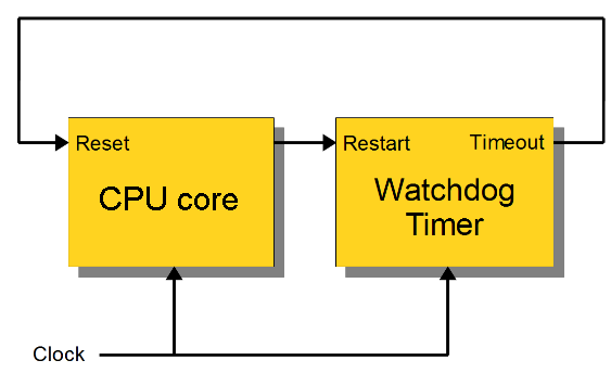
The Watchdog Timer (WDT) detects software faults by automatically generating a system reset or interrupt if the CPU fails to service the watchdog within a programmed interval.

WDT block diagram showing counter, interrupt, and reset output logic

  • Time-out mode: If the CPU does not restart the watchdog within the configured interval, the WDT asserts a reset signal to the ARM core.
  • Feeding the dog: Software must periodically write to WDT_CLR to restart the counter. Failure to do so within the interval causes a core reset.

WDT Interrupt

  • IRQn: 29

WDT Registers

Base address: 0x4004_1000

RegisterOffsetSizeTypeAccessDefaultDescription
WDT_VAL0x000032CRR/W0xFFFFFFFFCounter load value
WDT_CNT0x000432SRR0xFFFFFFFFCurrent counter value
WDT_CFG0x000832CRR/W0x00000000Configuration
WDT_CLR0x000C32ARWClear (feed) counter
WDT_INTRAW0x001032SRR0x00000000Raw interrupt status (unmasked)
WDT_INT0x001432SRR0x00000000Masked interrupt status
WDT_LOCKCR0x0C0032CRR/W0x00000000Register lock control
WDT_ITCR0x0F0032CRR/W0x00000000Internal test enable
WDT_ITOP0x0F0432CRR/W0x00000000Internal test operate

WDT_VAL — Counter Load Value Register

  • Address offset: 0x0000
  • Reset value: 0xFFFF_FFFF
BitsFieldDescription
[31:0]WDT_VALValue loaded into the counter. Write to set the timeout interval.

WDT_CNT — Counter Register

  • Address offset: 0x0004
  • Reset value: 0xFFFF_FFFF
  • Access: R
BitsFieldDescription
[31:0]WDT_CNTCurrent counter value (counts down)

WDT_CFG — Configuration Register

  • Address offset: 0x0008
  • Reset value: 0x0000_0000
BitsFieldDescription
[1]RSTReset enable: 1 = assert reset on timeout
[0]IRQInterrupt enable: 1 = generate interrupt on timeout

WDT_CLR — Clear Counter Register

  • Address offset: 0x000C
  • Type: AR (action register, write-only)
BitsFieldDescription
[31:0]Write any value to restart the watchdog counter (feed the dog)

WDT_INTRAW — Raw Interrupt Status Register

  • Address offset: 0x0010
  • Reset value: 0x0000_0000
  • Access: R
BitsFieldDescription
[31:0]Raw (unmasked) interrupt status

WDT_INT — Masked Interrupt Status Register

  • Address offset: 0x0014
  • Reset value: 0x0000_0000
  • Access: R
BitsFieldDescription
[31:0]Masked interrupt status

WDT_LOCKCR — Register Lock Control Register

  • Address offset: 0x0C00
  • Reset value: 0x0000_0000
BitsFieldDescription
[31:0]VALWrite 0x1ACE_E551 to unlock all WDT registers. Write any other value to lock them (registers become read-only). Bit [0] reads 1 when locked.

WDT_ITCR — Internal Test Configuration Register

  • Address offset: 0x0F00
  • Reset value: 0x0000_0000
BitsFieldDescription
[0]enInternal test mode enable

WDT_ITOP — Internal Test Operate Register

  • Address offset: 0x0F04
  • Reset value: 0x0000_0000
BitsFieldDescription
[1]irqGenerate watchdog IRQ (test mode)
[0]rstGenerate watchdog reset (test mode)